Wi-Fi weather station
Read a DHT22 or BME280 for temperature, humidity, and pressure, then push the values to a cloud dashboard like ThingSpeak or Blynk over Wi-Fi.
An open-source Wi-Fi development board built around the Espressif ESP8266EX, pairing a 32-bit microcontroller with 802.11 b/g/n networking on a breadboard-friendly module.
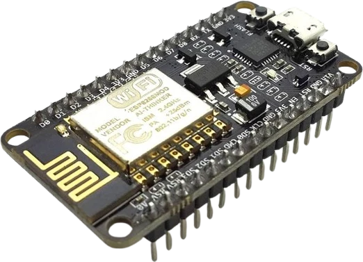
NodeMCU is a low-cost, open-source development board built around the Espressif ESP8266EX system-on-chip, carried here on the ESP-12E/12F module used by the LoLin V3 variant. It bundles a microcontroller and a 2.4 GHz Wi-Fi radio in a single package, so a single board can read sensors, run logic, and talk to the network without a separate shield.
At its core is a Tensilica Xtensa 32-bit LX106 RISC processor running at 80 MHz (configurable up to 160 MHz), backed by 4 MB of SPI flash and roughly 80 KB of usable RAM. The ESP8266EX implements a full 802.11 b/g/n WLAN MAC and TCP/IP stack. On the board, an AMS1117 regulator drops the 5 V USB/Vin rail to the 3.3 V the chip needs, and a USB-to-serial bridge (CH340 on LoLin units) handles programming and the serial console over micro USB.
Makers program it with the Arduino IDE (ESP8266 core), MicroPython, or Lua. The header layout exposes 11 usable GPIO, one 10-bit ADC channel, and hardware SPI, I2C, and UART, all on a 0.1 in pitch that straddles a breadboard. Its combination of price, size, and built-in Wi-Fi makes it a default choice for IoT sensor nodes, web-controlled gadgets, and cloud data logging.
| Pin | Function | Type |
|---|---|---|
A0 A0 (ADC0) | Analog single 10-bit ADC (TOUT), 0–1.0 V | Digital input |
RSV RSV | No connect | No connect |
RSV2 RSV | No connect | No connect |
SD3 SD3 (GPIO10) | Digital · PWM · SPI flash SDIO — usable as GPIO in DIO/QIO-safe modes | Bidirectional (GPIO) |
SD2 SD2 (GPIO9) | Digital · PWM · SPI flash SDIO — usable as GPIO in DIO/QIO-safe modes | Bidirectional (GPIO) |
SD1 SD1 (MOSI) | Digital GPIO8 · SPI flash MOSI (SDD1) — reserved | Bidirectional (GPIO) |
CMD CMD (CS) | Digital GPIO11 · SPI flash CS (SDCMD) — reserved | Bidirectional (GPIO) |
SD0 SD0 (MISO) | Digital GPIO7 · SPI flash MISO (SDD0) — reserved | Bidirectional (GPIO) |
CLK CLK (SCLK) | Digital GPIO6 · SPI flash SCLK (SDCLK) — reserved | Bidirectional (GPIO) |
GND GND | Power | Power in |
3V3 3V3 | Power | Power out |
EN EN | Digital chip enable (active-high); leave pulled up for normal run | Digital input |
RST RST | Digital active-low reset | Digital input |
GND_2 GND | Power | Power in |
VIN Vin (5V) | Power | Power in |
D0 D0 (GPIO16) | Digital GPIO16 — read/write + deep-sleep wake only; no interrupt/PWM/I²C/OneWire | Bidirectional (GPIO) |
D1 D1 (GPIO5) | Digital · PWM · I²C SCL (default Wire) | Bidirectional (GPIO) |
D2 D2 (GPIO4) | Digital · PWM · I²C SDA (default Wire) | Bidirectional (GPIO) |
D3 D3 (GPIO0) | Digital · PWM · Strapping FLASH button — hold LOW at reset to enter flash mode; HIGH for normal boot | Bidirectional (GPIO) |
D4 D4 (GPIO2) | Digital · PWM · UART TXD1 (debug) · Strapping on-module blue LED (active-low); must be HIGH at reset | Bidirectional (GPIO) |
3V3_2 3V3 | Power | Power out |
GND_3 GND | Power | Power in |
D5 D5 (GPIO14) | Digital · PWM · SPI HSPI SCLK (default SPI SCK) | Bidirectional (GPIO) |
D6 D6 (GPIO12) | Digital · PWM · SPI HSPI MISO (default SPI MISO) | Bidirectional (GPIO) |
D7 D7 (GPIO13) | Digital · PWM · SPI HSPI MOSI (default SPI MOSI) · UART RXD2 | Bidirectional (GPIO) |
D8 D8 (GPIO15) | Digital · PWM · SPI HSPI CS (default SPI SS) · UART TXD2 · Strapping must be LOW at reset for normal boot | Bidirectional (GPIO) |
D9 D9 (GPIO3/RX) | UART RXD0 (Serial RX) · Digital | Bidirectional (GPIO) |
D10 D10 (GPIO1/TX) | UART TXD0 (Serial TX) · Digital | Bidirectional (GPIO) |
GND_4 GND | Power | Power in |
3V3_3 3V3 | Power | Power out |
Verified from the Tinkered component library · LoLin.
The ESP8266 I/O is 3.3 V and is not 5 V tolerant. Wiring a 5 V logic output, sensor, or the Vin rail straight to a GPIO can permanently damage the pin or the chip. Level-shift or divide any 5 V signal first.
The silkscreen D-numbers do not match the GPIO numbers. D1 is GPIO5, D2 is GPIO4, D3 is GPIO0, and so on. Mixing them up in code (for example calling pinMode on the GPIO number instead of the Arduino D constant) drives the wrong pin.
GPIO0 (D3), GPIO2 (D4), and GPIO15 (D8) must be at the correct level at reset. Holding GPIO0 low, pulling GPIO2 low, or pulling GPIO15 high at power-up puts the board into flash mode or stops it booting. Reserve these pins for signals that idle in the safe state.
The AMS1117 regulator and the 3V3 rail have limited headroom, and Wi-Fi activity causes current spikes. Powering several sensors, a display, and a radio module all from 3V3 can cause brownouts and random resets. Budget the current and add decoupling capacitors.
The ADC input is rated to a low full-scale voltage (0 to 1.0 V on the bare chip). Applying more than the rated voltage to A0 gives clipped readings or damages the input. Scale higher voltages down with a divider sized for the actual range.
Read a DHT22 or BME280 for temperature, humidity, and pressure, then push the values to a cloud dashboard like ThingSpeak or Blynk over Wi-Fi.
Run a small HTTP server on the board so a phone browser can switch a relay, controlling lights or appliances from anywhere on the local network.
Publish sensor readings and subscribe to commands over MQTT, letting the board join a Home Assistant or Node-RED setup as a low-cost wireless endpoint.
Wire GPIO16 (D0) to RST and use deep sleep so the board wakes periodically, takes a reading, transmits it, and sleeps again to stretch battery life for weeks.
Expose the board's pins through a simple JSON REST API so other devices or scripts can read inputs and toggle outputs remotely.
Use the ESP8266 Arduino OTA library to push new firmware over Wi-Fi, so a deployed board can be reprogrammed without a USB cable.
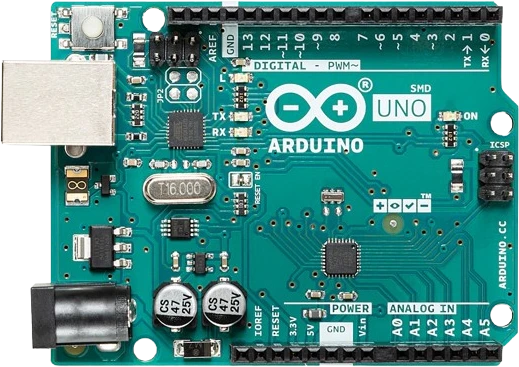
arduino-unoATmega328P · 5V logic
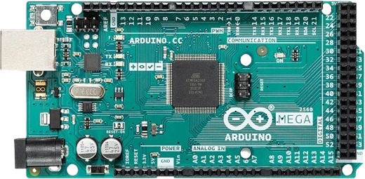
arduino-megaATmega2560 · Expanded I/O
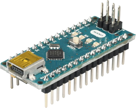
arduino-nano-v3ATmega328P · Compact format
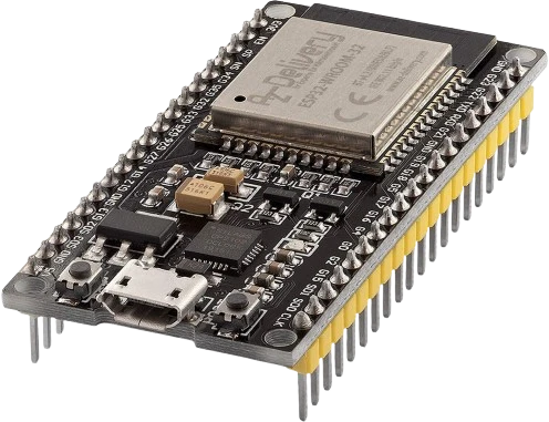
esp32-devkitWi-Fi + Bluetooth
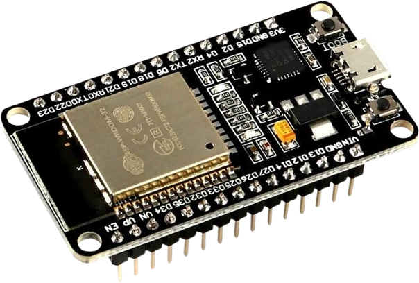
esp32-devkit-v1DOIT · 30-pin
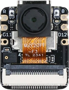
xiao-esp32-s3-senseCompact AI + wireless
Drop the ESP8266 NodeMCU into a circuit, write firmware, and simulate it in your browser, then deploy to real hardware. All in one editable Tinkered project.